
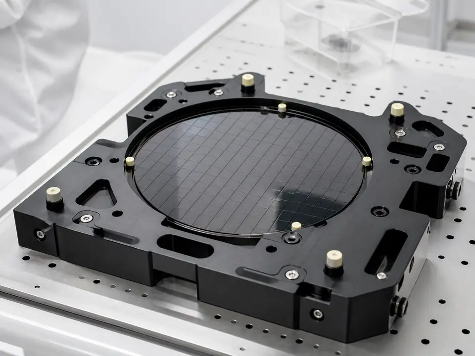
PEEK CNC Machining for Semiconductor Components
A representative engineering scenario for precision PEEK parts used in semiconductor equipment.
Project Overview
This anonymized scenario concerns a drawing-based PEEK equipment component requiring stable interfaces and controlled inspection. No customer identity or proprietary geometry is disclosed.
Engineering Challenge
The part combined thin features, critical mounting datums and material-performance requirements. Machining heat, workholding and dimensional movement needed consideration.
Materials
PEEK was selected for temperature capability, mechanical performance, chemical resistance and electrical properties. The exact resin grade and documentation package remain project-specific.
Manufacturing Process
Five-axis or multi-setup CNC machining can be planned around stable workholding, staged material removal and final critical-feature finishing. Inspection is aligned with functional datums.
Application
Potential applications include chamber components, insulating mounts, carriers, nests and equipment interfaces where PEEK properties match the documented operating conditions.
Quality Considerations
Inspection and quality review are planned according to drawing requirements, material behavior, tolerances, surface expectations and the intended application. No single inspection method is assumed for every project.
Related Capabilities
Frequently Asked Questions
No. The case studies are anonymized representative engineering scenarios and do not disclose customer identities.
Yes. STEP, STP, IGES, DXF, PDF and relevant reference files can support review.
Yes. CNC machining is well suited to prototypes and repeat low-volume production.
Request a Quote for Your Project
Send your drawing, image or reference file. Our engineering team will review the requirements and recommend a suitable manufacturing solution.
Material, Industry and Process Resources
Review the material, application and manufacturing resources related to this project example.
